
Semiconductor FOWLP/OSAT Equipment Business Consulting
As Moore’s laws shrinking does not bring traditional cost advantages anymore, semicon industry has turn to Advanced Packaging Heterogeneous Integration for the next few decades of More-than-Moore productivity gain. In the Advanced Packaging space, the leading technology is the Fan-Out Wafer level Packaging, FOWLP, which is deem one of the next enabling “embedding” integration technology that provides the “similar continuous scaling of IC System” features into a smaller and tinier scaling the package level to catch up with the ever demanding higher and higher system capabilities drive.
We were fortunate to have spotted this trend and has been the pioneer of the World-first more-than 300mm size Fan-out Wafer-Level Equipment know- how since 2009. With >10 years of FOWLP Equipment field experience, we have the know-how to achieved numerous Best-In-Class Productivity on the various FOWLP equipment processes tool and would be able to provide consulting service for both Equipment suppliers and end-users needs for higher productivity equipment.
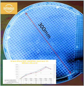 Do you know you can increase your wafer size to 330mm dia and process on normal 300mm wafer level equipment?And gain 20% to 25% real estate?
Our Best-In-Class innovative configuration of sputtering process tool in FOWLP helps to increase Thru-put by 10x from without Best-In-Class configuration tools. This Best-In-Class configuration has been adopted even by the world largest and most advanced foundry which has started historical moment of production of FOWLP in 2016 on the most desirable phone AP chipset.